
Charles R. Goulding and Fraser Lintott explore how additive manufacturing can improve the process of fabricating chips.
A Shift in the Industry
Moore’s Law, created in 1965, theorizes that the number of transistors on an integrated circuit, more commonly known as a microchip, doubles every 2 years, and for more than 50 years the theory has held true. Recently, however, Moore’s law has slowed down, with some even arguing its death.
Part of the reason for this is transistors have reached their atomic limit, making it increasingly difficult to shrink them. The other driving factor is cost. Moore’s Second Law or Rock’s Law states that every four years the cost of a chip fabrication plant doubles. Modern chip plants can cost up to 10-20 billion dollars, which is about a third of the 50 billion dollars President Biden has set aside for chip manufacturing in the US.
In search of increased computing power and reduced cost in light of recent chip shortages, researchers and manufacturers have shifted their focus towards chiplets.
What is a Chiplet?
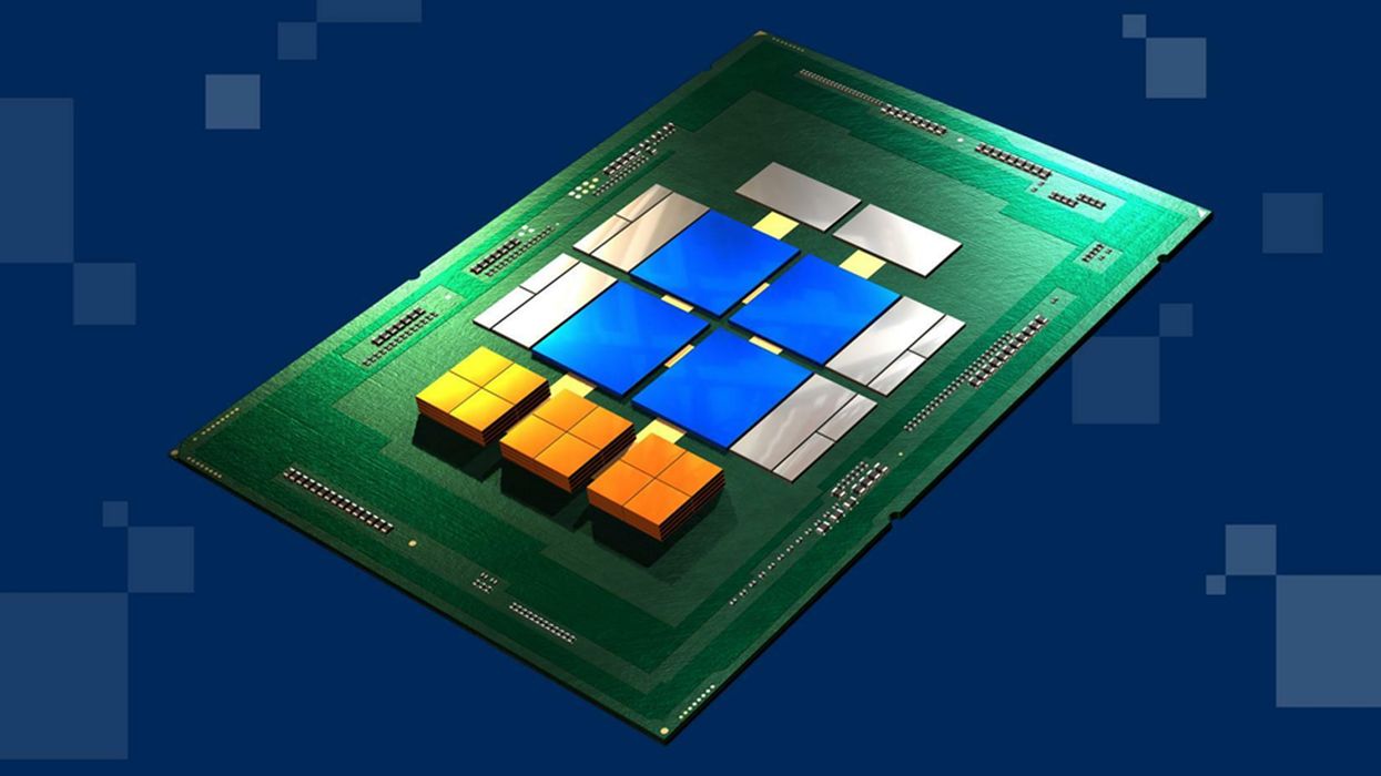
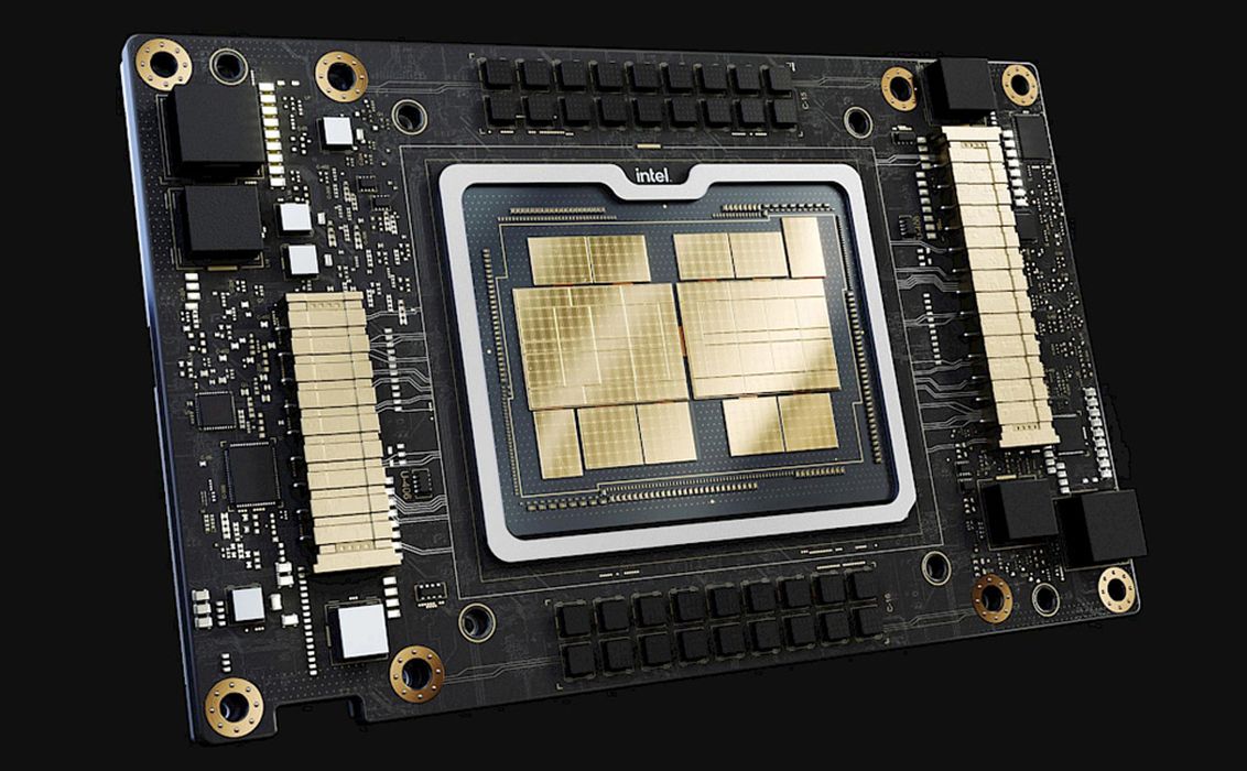
Rather than manufacturing a chip on a single substrate, chiplets utilize multiple small ICs (integrated circuits) specialized for distinct functions which make up a larger circuit. Heterogeneous integration technology allows these different chiplets to be mixed-and-matched as needed for different uses such as graphics and AI computation.
Advances in packaging are what make these advancements in chiplets possible. Chiplets can be organized in both two dimensions and three dimensions, stacking the chips on top of each other to position them as close as possible. Another key factor in the packaging of chiplets is the high-speed electrical connections between them.
Intel, AMD, and More
Due to their increased performance and decreased cost, chiplets have already been adopted by Amazon, AMD, Apple, IBM, Intel, and Tesla to name a few. In fact, according to the Yole Group, a market research firm, “as much as 80% of microprocessors will use chiplet-style designs by 2027”.
Intel’s recent use of chiplets is seen in their new processor, “Ponte Vecchio.” This chip is one of the most advanced with over 100 billion transistors. This GPU will give Argonne National Laboratory’s supercomputer, Aurora, over two exaflops of computing power. To put that into perspective, the computer can compute more floating-point operations in a single second than there are total seconds in the lifespan of every American.
AMD, Intel’s biggest competitor, does not plan to fall behind. Their own accelerated processing unit (APU) called the MI300 beats intel in transistors with 146 billion on the mega chip. They will also power a supercomputer at the Lawrence Livermore National Laboratory.
Additive Manufacturing
Unfortunately for the US, due to the labor-intensive process of packaging, much of the work has been exported to Asia. As packaging becomes increasingly important for the incorporation of chiplets, creating new domestic facilities becomes a greater priority.
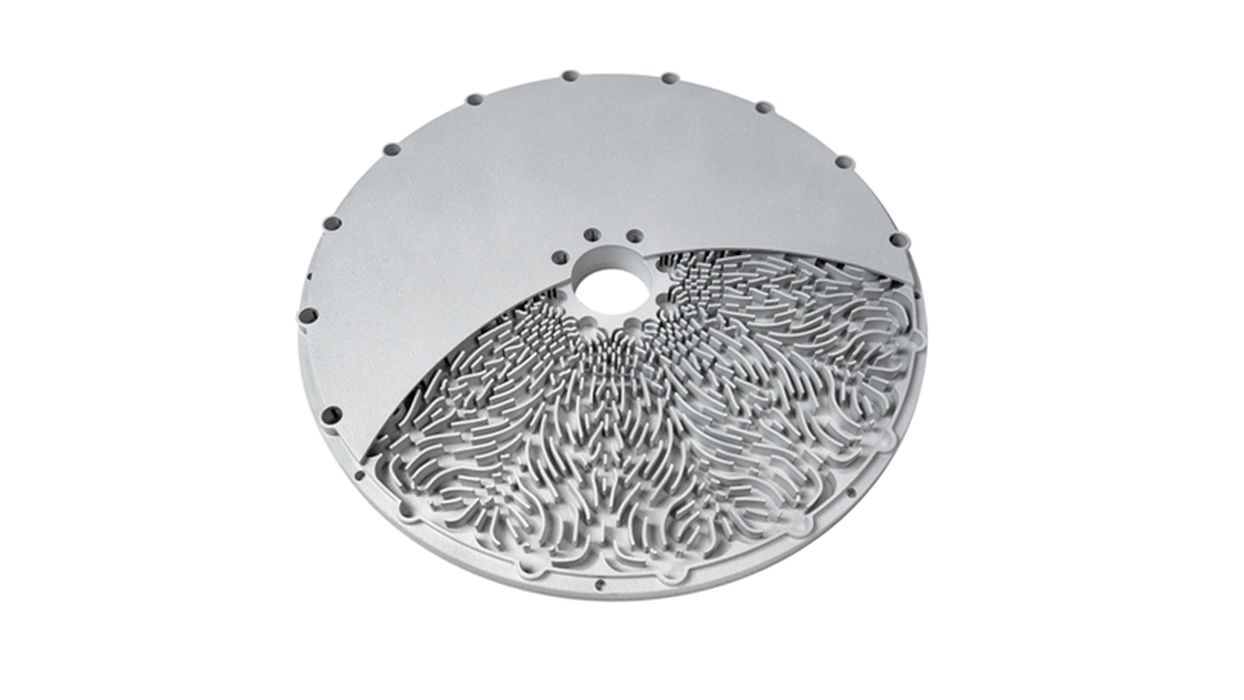
3D printing may be able to help. Chip fabrication parts are incredibly intricate requiring multiple parts to be brazed together. These parts can take months to make and any changes in their design can majorly affect project lead-time. Additive manufacturing creates monolithic parts which can manufactured faster and more accurately allowing for fewer manufacturing defects and increasing ROI.
The Research & Development Tax Credit
The now permanent Research and Development (R&D) Tax Credit is available for companies developing new or improved products, processes and/or software.
3D printing can help boost a company’s R&D Tax Credits. Wages for technical employees creating, testing and revising 3D printed prototypes can be included as a percentage of eligible time spent for the R&D Tax Credit. Similarly, when used as a method of improving a process, time spent integrating 3D printing hardware and software counts as an eligible activity. Lastly, when used for modeling and preproduction, the costs of filaments consumed during the development process may also be recovered.
Whether it is used for creating and testing prototypes or for final production, 3D printing is a great indicator that R&D Credit eligible activities are taking place. Companies implementing this technology at any point should consider taking advantage of R&D Tax Credits.
Conclusion
Chiplets provide a faster and cheaper option than monolithic chip manufacturing. With major global players in the global chip market switching their focus towards chiplets, it is clear that they will become the future of computing.