
Nano Dimension’s CEO invited me to drop by HQ for a look inside nanotechnology and electronics 3D printing.
While in Israel this week, I saw some wonderful things: XJet’s grand opening for its new Additive Manufacturing Center, the Dead Sea, Jerusalem, Masada, and printed circuit boards being 3D printed. This last was a welcome, unplanned addition to my dedicated Israeli excursion, and as it turns out there was simply no better way to close out a business trip rooted in history and focused on innovation.
The history in Israel is all around, in every rock and cave – and in every science park. The area around Ness-Ziona Science Park has long been home to innovation in inkjet printing, and has deep roots for 3D printing. Nano Dimension is built upon this long legacy in additive manufacturing, as its co-founders bring great experience to bear in this young endeavor.
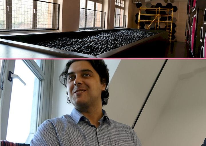
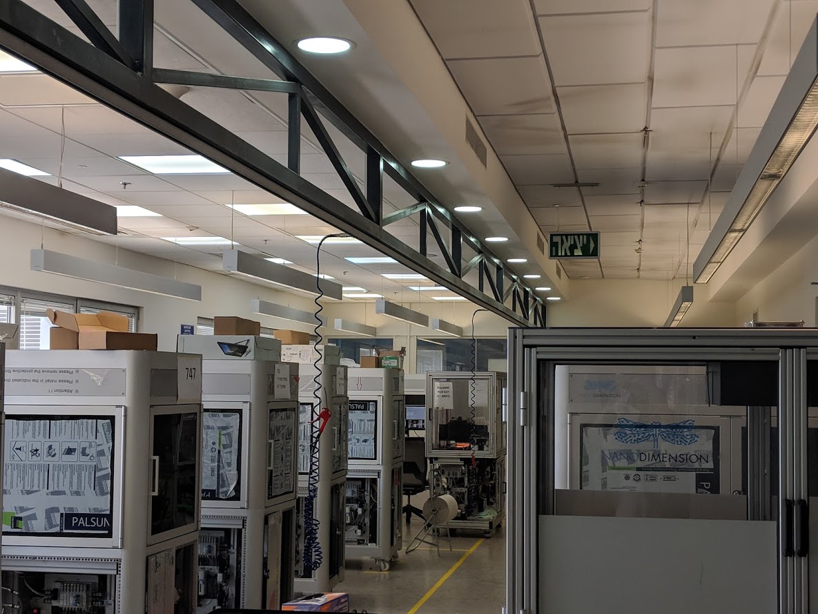
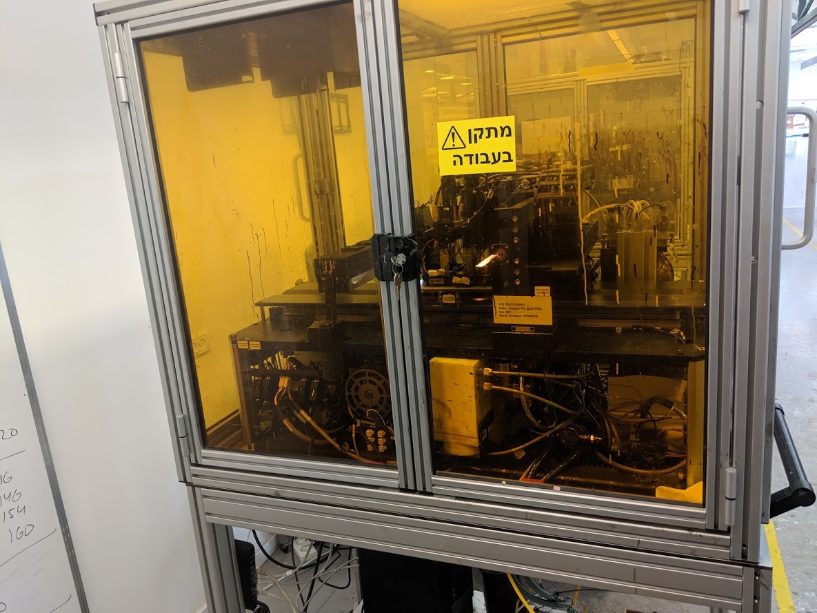
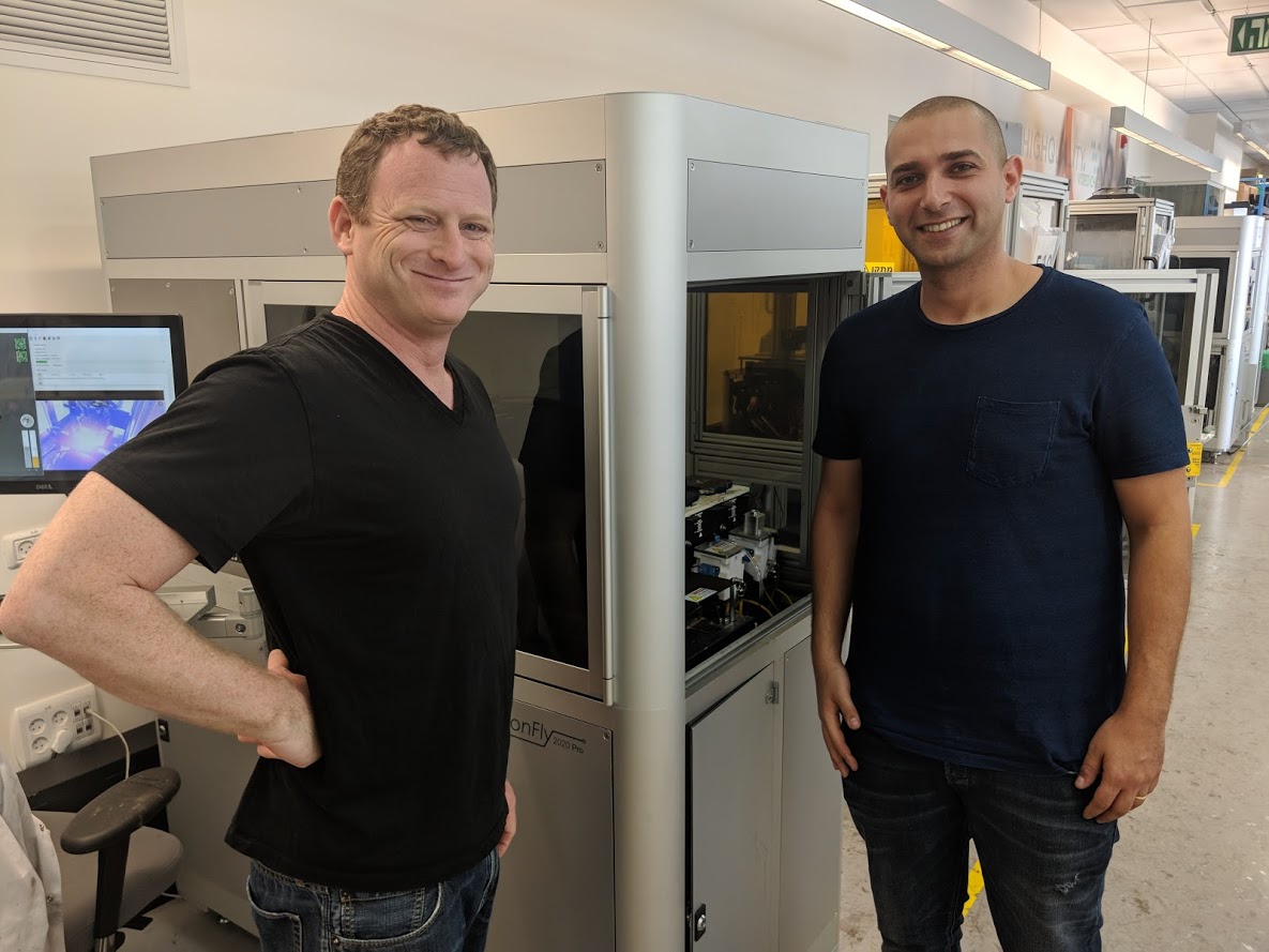
The headquarters spans three floors, and CEO Amit Dror was kind enough to show me through them, from conference rooms to manufacturing operations to the company’s first Customer Experience Center. Following a quick chat about the area’s history – it’s a Mecca for inkjet, Dror noted as we chatted with Marketing and Public Relations Manager Galit Beck – we went to see where the DragonFly Pro 3D printers come together.
When it comes to electronics, precision reigns. This ethos spans the production process, as Dror explained:
“It’s electronics. We have to meet the standards. The process has to be perfect at all times, there is no point at which we can let that go with electronics. We require complete precision throughout.”
Sales, he continued as we walked around the machines in the process of being built from initial (very precise) assembly to initial wetting with inks, are increasing and increasing. The challenge for the next year is a tough but appreciated one: how to ramp up production.
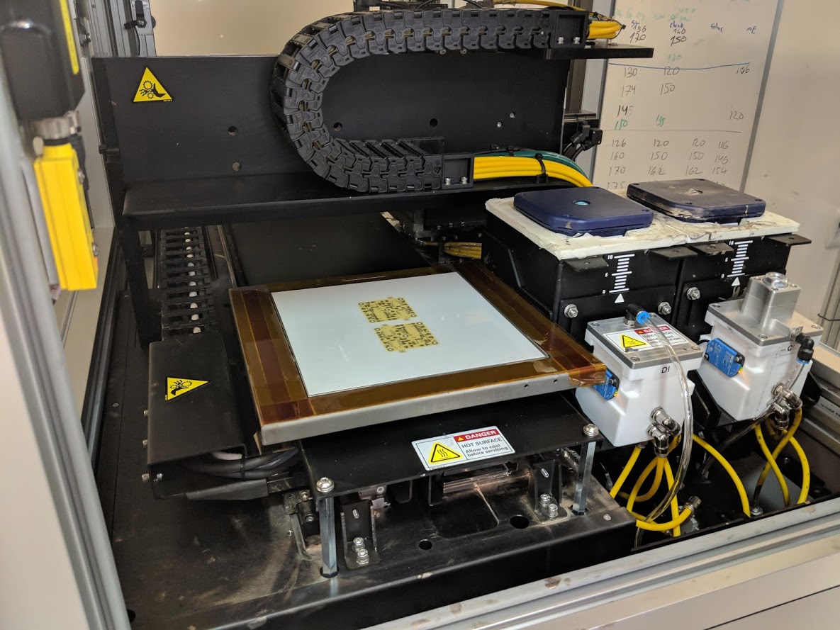
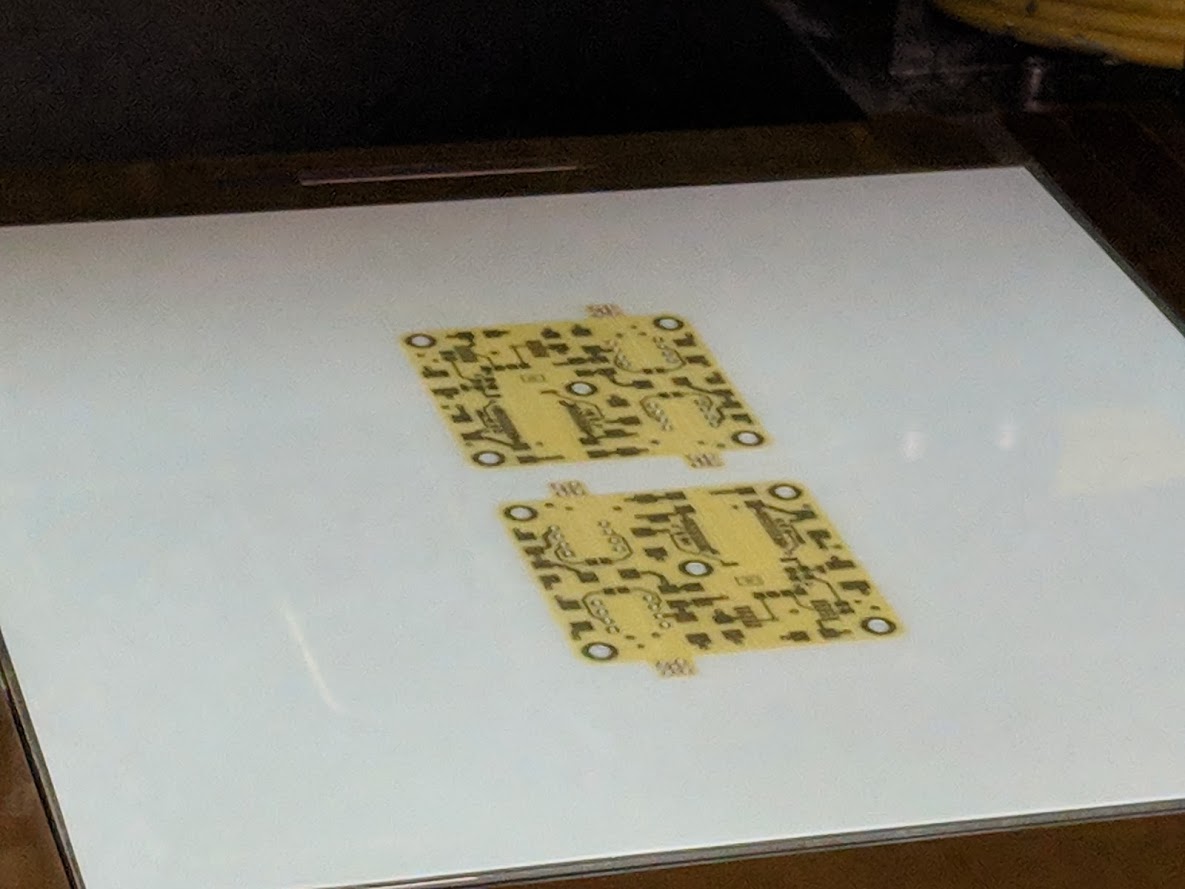
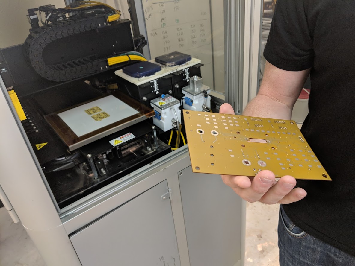
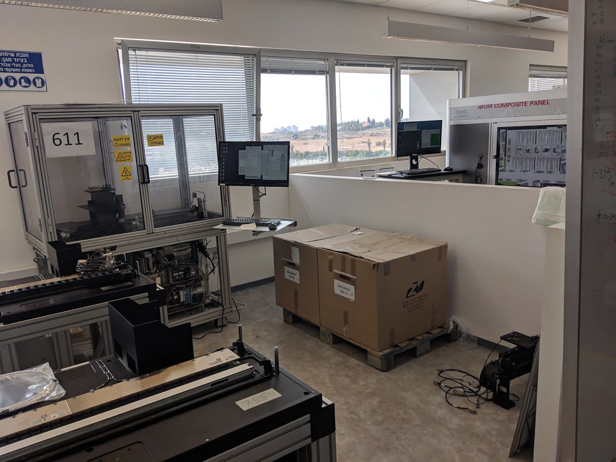
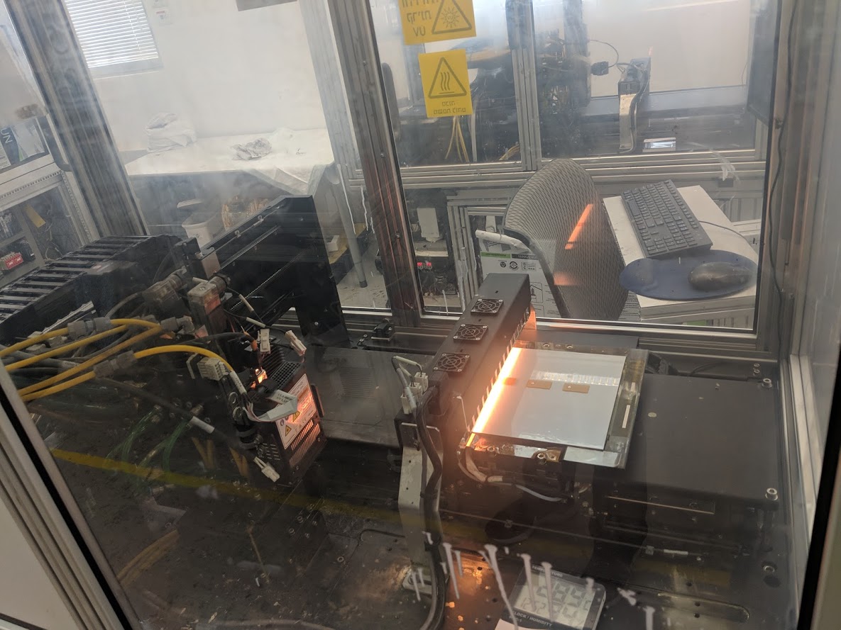
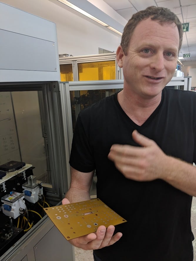
We spoke with R&D Integration Team Leader Yoav Rozanovich for a closer look at all that goes into the process for a finished DragonFly Pro unit, as he and Dror walked me through the step-by-step (layer-by-layer) process of electronics 3D printing. Each layer of a printed circuit board (PCB) is essentially designed in 2D, and can be done in the program of the designer’s choice; these are then uploaded into Nano Dimension’s Switch software, which works with the overall .gbr file to create the multi-layered structure with both conductive and non-conductive (dielectric) inks.
“We use polymer ceramic material and a metallic, silver material,” Dror noted as we watched an in-process build. “These materials don’t like to be together, so we try to make peace between the families. This is what differentiates us, as we take this to a level allowing them to sit comfortably and support professional electronic capabilities.”
For the multi-material build to work properly within a single build chamber, the materials must be laid down within the same settings range. The polymer, however, likes temperatures around 60C, while the silver likes a range closer to 300C, Dror said. But for this process, it’s not about melting the silver; it’s about controlling it.
This, Dror continued, is why Nano Dimension has “nano” in the name: they’re working with nanomaterials.
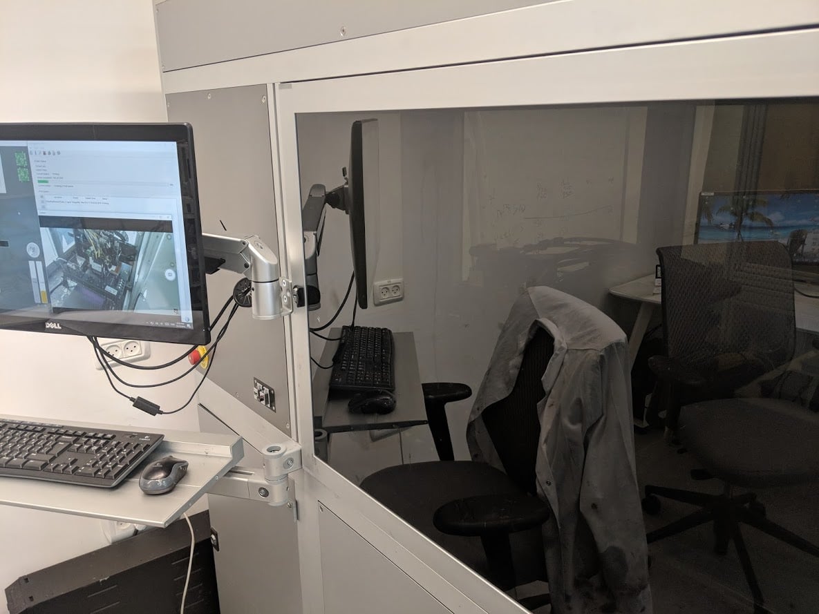
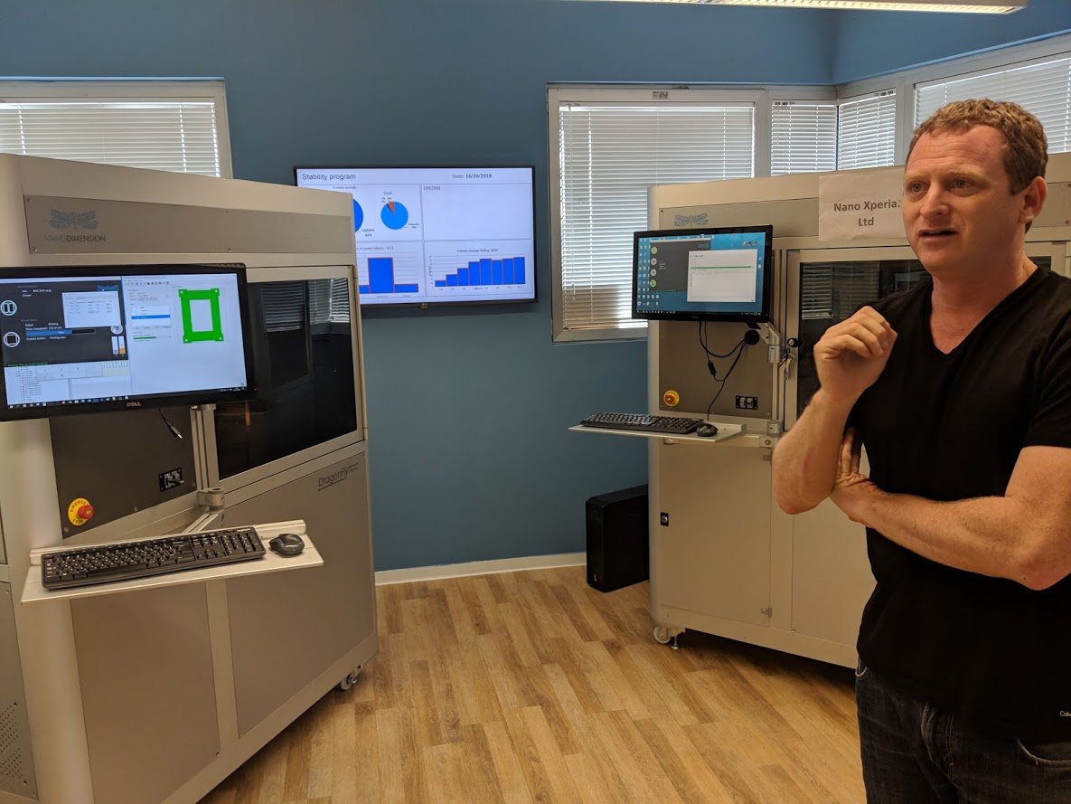
We continued the conversation as we moved into the Customer Experience Center (CEC), where two production-ready DragonFly Pro units showcase their capabilities. One runs for “Nano Xperia Ltd.”, a “customer” case that the company uses to hone in on exactly how to respond to users’ needs by bringing non-technical employees from Nano Dimension and treating them as users.
“What’s intuitive for technical people many not be intuitive for non-technical people; this shows us how to improve and educate,” Dror said.
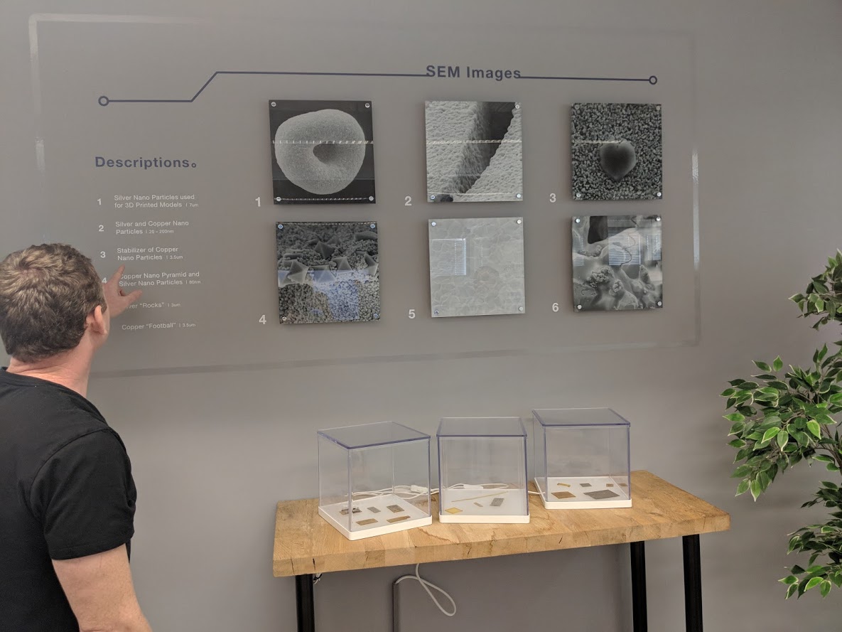
Opposite the machines are massively magnified images of the nanomaterials Nano Dimension uses in its PCB creation. Looking closely at the structures shows how complex their makeup is and leads to more appreciation for the control the company is able to exert over them to create functional electronics.
“To introduce a product is one thing; carving to the heart of production is a second thing. When you see a full-color 3D printed heart, for example, it’s amazing. For us, though, it’s all about functionality. For us to go to our customers’ mainstream, we have to help with production,” Dror explained.
“We’re in 3D printing, and it’s like a bubble – it’s really cool. We need to go beyond that for production.”
A major focus here is MTBF (mean time between failures) and MTBI (mean time between interrupts), which are terms common in manufacturing but not yet so common in 3D printing. A study of Nano Xperia’s experiences details the MTBF as the company tracks progress in uptime to get a better sense of how to reduce downtime – a critical consideration for production applications.
As we moved into the R&D lab, Dror continued to discuss the markers of success when it comes to 3D printing in the electronics industry, which transcend into larger trends in additive manufacturing.
“To get it right, it’s not just about the printer, it’s not just about the material, it’s not just about the software, it’s not just about the process. It’s really everything needs to be in place, it’s very complex and it all needs to work side by side,” he explained. “The higher the complexity is, the riskier it is to not get it right. This is a complex multi-disciplinary effort, and so we put everyone together.”
Software engineers and chemists may not always speak the same language, but here they are working together with real understanding. One of the biggest facets of Nano Dimension that came up time and again through speaking with Dror, Beck, and Rozanovich was that multi-functionality: the team deeply values being a team. Communication across disciplines, and between floors of work space, is keeping the innovative spirit going and keeping the company culture true to its roots.
These roots come down to four major company values:
-
Innovation
-
Openness/Collaboration
-
Accountability
-
Execution
If there were to be a fifth, it would be balance. Creating a balanced ecosystem and a balanced work environment is integral to the ongoing success of the company. The team is about 100 strong today, and notably includes a diverse range of employees (also notably, every chemist in the labs during my walkthrough was female).
“We have an open atmosphere; it’s very unique here. It’s more than collaborating,” Beck said as we sat down and chatted over coffee.
Members of each team are welcome to contribute, and have proven comfortable doing so, to efforts across the company.
“If it wasn’t for that, we wouldn’t be able to overcome the challenges we see every day, coming in from the window and from the door,” Dror added. “People feel free to collaborate and work together.”
To date, Nano Dimension has produced around 50 machines at this site. Operations are expanding globally, with offices in the US (Nano Dimension’s largest market) and in Hong Kong to support burgeoning sales across North America, Europe, and the Asia Pacific region. The company works with resellers in each area (“There’s no way we could do it all ourselves,” Dror said with a smile) and continues to look forward.
The growth potential on-site at Nano Dimension is palpable. With accomplishments in production and sales already documented, and much of the office space still looking fresh and new, the young company is already eyeing its next phases of growth. Hiring is ongoing, and there’s already talk of how to house expanded production operations.
We’ll be keeping up with the team for upcoming closer looks into use cases that will be going public in the not-too-distant future, and look forward to seeing them again in a few weeks at formnext. Not all of them, though; Nano Dimension is keeping very busy, now attending about 10 events globally each quarter, and while formnext represents a major hive of activity in additive manufacturing, the like-timed Electronica show will be more of a draw for this company’s user base. Formnext is absolutely a valuable show in the 3D printing industry, and our team are very much looking forward to it. It does still represent something of a bubble, though, with all eyes on additive there. Just as at this year’s IMTS there was 3D printing in every hall, including well away from the dedicated AM Pavilion, which highlighted the growing rates of adoption and proven applicability in manufacturing, seeing more 3D printing at not-3D printing events showcases the expansion of usage across targeted verticals.
Visiting Nano Dimension this week has provided some excellent food for thought in terms of applications, materials science, conscientious growth strategies, and global expansion. Our thanks to the team for their invitation and hospitality.
Via Nano Dimension
[All images: Fabbaloo]