
Charles G. Goulding highlights how pioneering advancements in photonics manufacturing can be enhanced with 3D printing and qualify for substantial R&D tax incentives.
Photonics: Why Engineers Keep Returning to Light
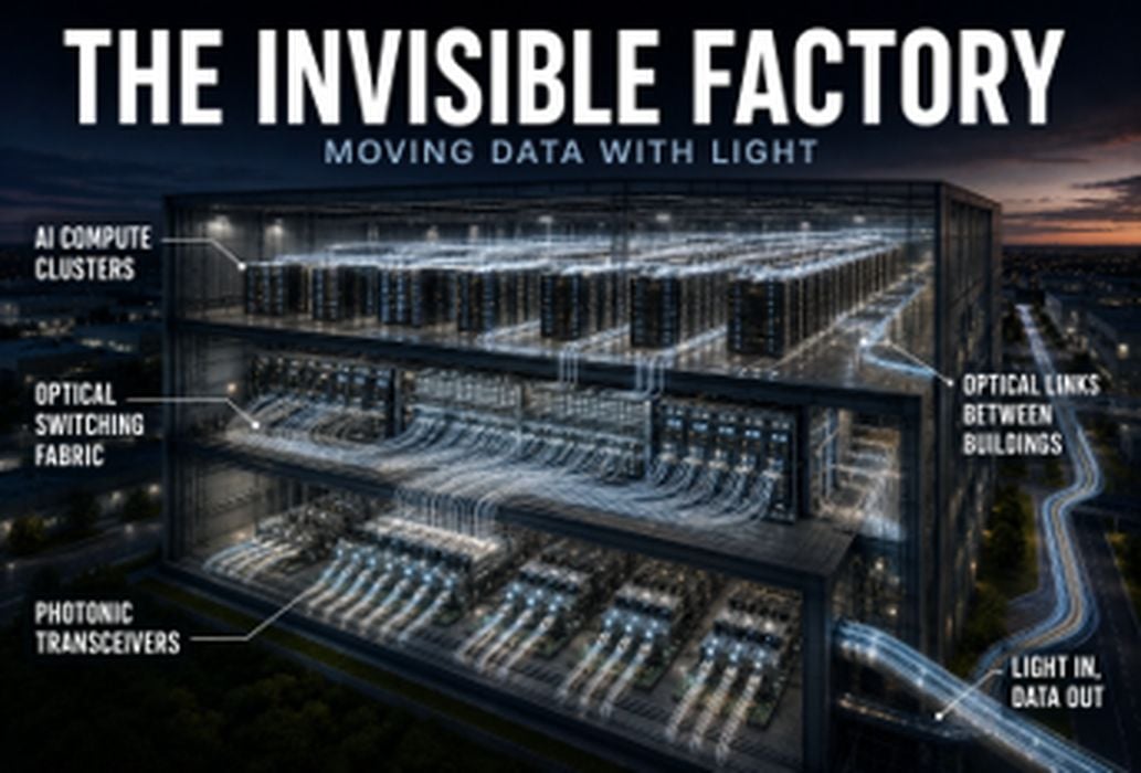
A modern AI cluster spends much of its life moving information.
Processors complete calculations in fractions of a second. The next calculation often depends on data arriving from somewhere else. Information travels between GPUs, memory systems, storage devices, and networking equipment. As computing systems grow larger, the movement of information becomes as important as the calculations themselves.
Engineers usually attack that problem electronically. Faster processors increase the amount of information moving through the system. That additional traffic places pressure on networking hardware, packaging, and power delivery. Eventually the effort required to move information begins competing with the effort required to process it.
That is often when engineers return to light.
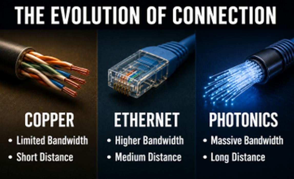
Photonics is the science and engineering of generating, controlling, and transmitting light. Telecommunications encountered the challenge decades ago. Networking systems encountered it next. Large-scale AI infrastructure now faces similar pressures because light can carry enormous amounts of information while avoiding some of the penalties associated with moving information electronically.
Systems grow larger. Distances increase. Data volumes expand. With the help of modern photonics, engineers are finding new pathways given these developments.
Inside the Photonic Device
An optical transceiver occupies surprisingly little space. Most fit comfortably in the palm of a hand.
Yet those small devices help move information through some of the largest computing systems ever assembled. Open one and the interior looks more like a scientific instrument than a traditional computer component.
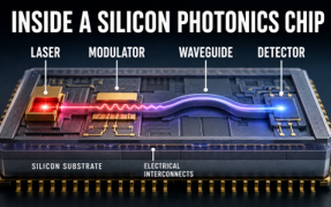
A laser generates the signal. The rest of the device exists largely to preserve that signal as it travels through increasingly small and precise structures. Light must follow carefully controlled paths before eventually being converted back into an electronic signal. The process sounds straightforward until components shrink and manufacturing tolerances tighten.
The physical reality of what really transpires often surprises people. The performance of a massive computing system can depend on components smaller than a fingertip.
Coherent operates in this world through optical networking products, lasers, materials, and photonic systems. The company’s fiscal 2025 materials describe markets that span communications, industrial systems, instrumentation, and electronics. The hardware may be small, but consequences are not.
3D Printing Photonic Components
A photonic device often succeeds or fails because of geometry.
Light must travel through carefully controlled pathways. Keeping those pathways aligned becomes harder as devices shrink and thermal loads increase. Heat that appears insignificant elsewhere can alter performance inside a photonic system.
Those requirements have created opportunities for additive manufacturing. Nanoscribe has developed micro-scale 3D printing systems capable of producing optical components measured in microns.
Researchers use the technology to fabricate miniature lenses and optical structures that would be difficult to manufacture through conventional methods. The resulting components often look less like traditional manufactured products and more like tiny pieces of laboratory equipment.
Conventional manufacturing struggles when optical features become measured in microns because the tolerances approach the scale of the structures themselves. A component that appears simple under a microscope may contain features small enough that tiny manufacturing variations affect optical performance. Nanoscribe’s work on printing micro-optics directly onto optical fibers shows why alignment becomes so important when the optical surface and the fiber core must meet at submicron scale.
The same pattern appears elsewhere. UpNano’s high-resolution two-photon polymerization systems are used for micro-optics, chip-scale optical sensing, and interconnects for photonic integrated circuits or optical fibers. Fraunhofer IOF has developed inkjet printing approaches for three-dimensional optical elements and functional materials. Researchers have also demonstrated additive manufacturing for optical waveguides, where the printed geometry directly influences how light travels through the device.
Thermal management creates another challenge. Optical hardware generates heat. The resulting temperatures can affect alignment, performance, and reliability. Engineers increasingly use additive manufacturing to create cooling structures with internal passages that would be difficult to machine conventionally. Those designs help move heat away from sensitive components while occupying less space inside increasingly compact devices.
A printed structure can replace multiple brackets, mounts, and cooling components. Fewer interfaces reduce assembly complexity. Fewer components reduce opportunities for failure. The manufacturing process begins influencing performance before the device is even powered on.
In short, hurdles in photonics include:
- Submicron Alignment:
Optical transceivers require lasers, modulators, waveguides, and detectors to be integrated onto a single silicon substrate. Aligning a printed optical surface to a fiber core requires submicron-scale precision where minor geometric variations degrade optical performance.
- Thermal Distortion:
Optical hardware generates significant heat. In compact devices, even slight thermal expansions shift mechanical alignments and alter light pathways, requiring advanced, internal multi-passage cooling structures.
- Geometric Complexity:
Traditional manufacturing methods cannot produce the micro-scale lenses and optical structures required. Engineers are turning to additive manufacturing (such as two-photon polymerization and micro-scale 3D printing) to fabricate complex components measured in microns.
NVIDIA’s Investment in Coherent
A modern AI deployment may contain tens of thousands of optical links.
The processors receive most of the attention. The optical infrastructure determines how effectively those processors work together. Every delay leaves hardware waiting. Every bottleneck leaves expensive computing power underutilized.
That challenge helps explain NVIDIA’s investment in Coherent. NVIDIA agreed to invest US$2 billion in the photonics company as part of a broader multiyear partnership focused on advanced optics technologies, manufacturing expansion, and future AI infrastructure. The agreement also included a multibillion-dollar purchase commitment and future access and capacity rights for advanced laser and optical networking products.
The size of the investment attracted attention. The structure of the deal may be more revealing. NVIDIA was not simply purchasing components. It was helping expand the manufacturing capacity needed to produce them. The company effectively identified photonics as a potential bottleneck in future AI infrastructure and decided to invest accordingly.
The companies described the rationale directly: “Optical interconnects and advanced package integration are foundational to the next phase of AI infrastructure, as they unlock ultrahigh-bandwidth, energy-efficient connectivity across AI factories.”
Coherent occupies an unusual position within that ecosystem. The company manufactures optical networking products used inside AI infrastructure. It also produces industrial lasers, semiconductor equipment, communications technologies, sensing systems, and medical photonics products. Its 2025 financial results reflected strong demand connected to AI datacenter infrastructure.
Communications hardware represents only part of Coherent’s business, however. The same engineering principles that move information through an AI cluster also appear in factories, hospitals, research laboratories, and manufacturing systems. Following those applications provides a clearer picture of how widely photonics has spread across modern industry.
Photonics Beyond AI: Application 1 — Building With Light
A modern turbine blade contains a network of internal cooling passages hidden inside the metal.
Air moves through those passages while the engine operates at temperatures that would otherwise damage the component. Manufacturing those geometries has never been easy because many of the most important features are located where conventional tools cannot easily reach.
Lasers help change that equation. A laser can deliver energy to a highly specific location. That precision makes laser cutting, laser welding, and metal additive manufacturing practical for applications where conventional manufacturing struggles. Engineers have now gained the ability to create geometries that were previously expensive, difficult, or impossible to produce.
Rocket nozzles create another challenge. Internal channels, cooling structures, and weight constraints push engineers toward geometries that are difficult to manufacture conventionally. NASA work on channel-wall nozzles and additively manufactured combustion-chamber hardware shows how laser powder bed fusion and related processes can produce aerospace structures with internal cooling features that are difficult to make by traditional methods.
Inside a metal 3D printer, a laser moves across a bed of powder and melts material one layer at a time. The process repeats thousands of times until a finished component emerges. The laser is not communicating information. It is physically building an object.
Coherent’s industrial laser business operates in this environment. The company supplies laser sources and systems for cutting, welding, marking, ablation, semiconductor equipment, display manufacturing, precision manufacturing, and scientific research. The same company helping move information through AI infrastructure also supplies technologies used to manufacture aircraft components, automotive parts, medical devices, and industrial equipment.
Photonics Beyond AI: Application 2 — The Factory That Sees
A factory produces 10,000 metal components during a shift.
One machine gradually drifts out of alignment. The error is small enough that nobody notices immediately. Parts continue moving down the line. Boxes are packed. Trucks leave the facility. The problem is discovered days later when customers begin reporting failures.
Manufacturing spent much of the twentieth century operating this way. Parts were produced first and inspected later. Defects were often discovered after production stopped or after products reached customers. The delay increased costs because the factory had already consumed material, labor, and machine time before discovering something had gone wrong.
Optical systems changed that equation. Cameras, lasers, and sensors allow manufacturers to observe production while it is happening. Instead of asking whether a finished product meets specifications, factories increasingly ask whether the process itself remains within specifications.
The distinction is crucial because visibility changes behavior. A defect detected during production may require nothing more than a machine adjustment and a small amount of scrap. The same defect discovered after shipment can trigger warranty claims, replacement orders, customer complaints, and production delays. Information becomes more valuable when it arrives earlier.
Modern monitoring systems increasingly generate production histories rather than simple pass-fail decisions. Engineers can trace defects back to specific machines, materials, or process conditions. The factory gains the ability not only to detect problems but also to understand where those problems originated.
Many advanced metal printers now contain optical monitoring systems that watch each layer as it forms. Oak Ridge National Laboratory has described laser powder bed fusion as a process in which a high-energy laser melts successive layers of metal powder while inspection methods increase confidence in the printed part. Recent research on high-fidelity optical monitoring of laser powder bed fusion has examined whether in-process sensing can detect defects before downstream testing.
Companies such as Coherent participate here through sensing technologies and related optical systems. Coherent’s VCSEL materials describe sensing use cases ranging from optical computer mice and gaming systems to smartphone facial recognition, automotive sensing, and 3D sensing. The same underlying ability to generate, direct, and detect light supports industrial monitoring as factories gather information while production is underway.
Factories once depended primarily on machines that performed. Increasingly they depend on machines that can observe as well.
Photonics Beyond AI: Application 3 — Photonics in the Operating Room
A surgeon cannot operate on what cannot be seen.
That simple constraint explains why optical technologies appear throughout modern medicine. Endoscopes allow physicians to reach areas that would otherwise remain difficult to observe. That visibility creates opportunities for diagnosis and treatment that depend on accurate imaging. Cameras and related optical systems extend that visibility into increasingly specialized procedures.
Visibility changes what becomes possible. Better imaging can improve diagnosis. Better visualization can likewise improve surgical precision. The optical systems surrounding a procedure often influence outcomes long before the first incision is made.
Laser-based procedures provide another example. Light can be used not simply to observe tissue but to interact with it. Ophthalmology, dermatology, dentistry, oncology, and other specialties have incorporated photonic technologies because they allow physicians to deliver energy with extraordinary precision.
Medical photonics represents another market where companies such as Coherent apply the same optical principles found elsewhere in the industry. Coherent describes lasers, optics, delivery fibers, and components used in medical systems ranging from surgical lasers to dermatology and aesthetic systems. Its life-sciences materials also discuss imaging applications such as endoscopy and optical coherence tomography.
Medical-device manufacturers increasingly use 3D printing for custom instruments, specialized housings, and patient-specific products. The manufacturing techniques discussed in factories and data centers often reappear in hospitals.
Summary: Broad Industry Applications of Photonics
The engineering principles governing light transmission extend far beyond data centers into several multi-billion-dollar industries:
1. Aerospace and Industrial Manufacturing
High-energy lasers are used in laser powder bed fusion (metal 3D printing) to build complex components like rocket nozzles and turbine blades. Lasers melt material layer-by-layer to create internal cooling channels that are impossible to machine using conventional tooling.
2. Automated Factory Inspection
Instead of post-production testing, modern factories use in-process optical monitoring. High-fidelity cameras, Vertical-Cavity Surface-Emitting Lasers (VCSELs), and 3D sensors inspect components in real time, detecting micro-defects during the fabrication process to eliminate scrap and warranty claims.
3. Medical Photonics and Life Sciences
Surgical lasers, endoscopes, and optical coherence tomography (OCT) systems utilize precise light delivery to improve visualization and surgical accuracy. Medical device manufacturers also leverage micro-additive manufacturing to produce patient-specific surgical instruments and specialized optics housings.
How Photonics Engineering Qualifies for the R&D Tax Credit
The technological advancements, manufacturing scale-ups, and experimental designs occurring across the photonics sector directly align with the Federal Research and Development (R&D) Tax Credit. Companies designing, testing, or integrating optical components can claim a credit typically ranging from 4% to 7% of eligible spending.
The Four-Part Qualification Test
To qualify for the R&D Tax Credit, photonics projects must satisfy four specific criteria:
- Permitted Purpose (New or Improved Business Component): The work must intend to develop or improve the performance, reliability, quality, or efficiency of a product, process, software, or technique (e.g., designing a smaller silicon photonics chip or optimizing an optical transceiver package).
- Elimination of Uncertainty: The project must encounter technical uncertainty at the outset regarding the capability, methodology, or final design of the component (e.g., determining if a 3D-printed micro-lens can maintain submicron alignment under high thermal loads).
- Process of Experimentation: The engineering team must evaluate one or more alternatives to overcome the uncertainty through modeling, simulation, systematic trial-and-error, or prototyping (e.g., testing different internal cooling passage geometries in an optical housing).
- Technological in Nature: The research must fundamentally rely on principles of physical science, biological science, engineering, or computer science (e.g., laser physics, materials science, and optical engineering).
Eligible R&D Expenditures for Tax Savers
Photonics companies and AI infrastructure developers can include the following qualified expenses to offset their tax liabilities:
- Wages: Salaries paid to U.S.-based optical engineers, materials scientists, software developers, and QA technicians involved in testing prototypes.
- Supplies: Materials consumed during the prototyping and experimental fabrication phases, including silicon substrates, specialized lasers, and 3D printing resins.
- Contract Research: Fees paid to U.S. universities, laboratories, or third-party engineering firms conducting specialized optical testing or thermal modeling.
- Patent Costs: Legal and administrative expenses incurred while filing patents for novel photonic structures or manufacturing methodologies.
Startup & Small Business Incentives: Under the PATH Act, pre-profitable and pre-revenue startup businesses with less than US$50 million in revenue can use the R&D tax credit to claim up to US$500,000 per year in payroll tax offsets, turning non-refundable credits into immediate cash rebates
Below is a table that presents the recent R&D spend incurred by Coherent as compared to its human capital.
| Coherent Photonics LLC | ||||
| Book per Capita R&D Expenses | ||||
| Company | Year | R&D Expenses (USD) | Number of Employees | R&D Expenses per Employee |
| Coherent | 2025 | 581,920,000 | 30,216 | 19,259 |
| 2024 | 478,790,000 | 26,157 | 18,304 | |
| 2023 | 499,600,000 | 26,622 | 18,766 | |
| 2022 | 377,110,000 | 23,658 | 15,940 | |
Below is a table that illustrates the core technologies and primary R&D challenges for the industry.
| Sector | Core Technology | Primary R&D Challenge / Qualifying Activity |
| AI Clusters | Silicon Photonics & Transceivers | Minimizing signal degradation and maximizing bandwidth at submicron scales. |
| Industrial Lasers | Powder Bed Fusion Additive Mfg. | Controlling energy delivery to form complex internal geometries without structural defects. |
| Factory Inspection | VCSELs & 3D Sensing Systems | Developing real-time, high-fidelity optical monitoring algorithms to detect micro-faults. |
| Medical Devices | Surgical Lasers & OCT Imaging | Engineering ultra-precise beam delivery systems and bio-compatible miniature optics. |
Building Optical Hardware at Scale
An AI cluster may require thousands of optical modules. A factory producing a few hundred per month has a problem.
The growth of AI infrastructure has created demand for enormous quantities of photonic hardware. Components that once looked specialized now behave more like industrial infrastructure. As deployments grow larger, optical hardware begins facing many of the same manufacturing pressures as transformers, cooling systems, and other critical equipment.
That pressure helps explain why NVIDIA’s partnership with Coherent focused on manufacturing capacity as much as technology. The challenge was not simply inventing better optical hardware. The challenge was producing enough of it.
Every optical module combines multiple optical and electronic systems inside a package that must perform consistently over long operating periods. The challenge grows as production volumes increase because manufacturing variations that are manageable in prototypes become costly at industrial scale.
| Where Photonics Appears | What the Technology Does |
| AI Clusters | Moves information between computing resources |
| Industrial Lasers | Delivers energy to manufacture parts |
| Factory Inspection | Detects defects during production |
| Medical Devices | Improves visibility and precision |
| Scientific Equipment | Measures and analyzes physical phenomena |
The challenge resembles earlier periods in semiconductor history. Designing a better chip mattered. Producing millions of reliable chips mattered just as much. Photonics increasingly appears to be entering a similar phase. Competitive advantages are beginning to emerge not only from design but from manufacturing scale.
If photonic technologies continue moving into new markets, many of the building blocks already exist. Photonics keeps connecting them. The same company supplying optical hardware for AI clusters also supplies technologies used to manufacture parts, inspect factories, and support medical procedures. As computing systems continue pushing against physical limits, the demand for moving information efficiently is unlikely to disappear. Engineers have spent decades responding to that challenge with light.
Charles G. Goulding is a practicing attorney.
Frequently Asked Questions
Why is NVIDIA investing billions of dollars in photonics?
NVIDIA invested US$2 billion in Coherent because optical infrastructure is the primary bottleneck in scaling next-generation AI data centers. Without advanced optical transceivers, high-speed GPUs waste processing cycles waiting for electronic data transfers.
How does micro-3D printing benefit optical engineering?
Technologies like two-photon polymerization allow manufacturers to print micro-optics directly onto optical fibers. This eliminates traditional assembly steps and ensures the submicron structural alignment required to prevent light signal loss.
Can electronics manufacturing companies claim R&D tax credits for optical integration?
Yes. Any company designing processes to transition from electronic data transfer to optical data transfer faces technical uncertainties regarding thermal management, component placement, and signal integrity. The engineering hours and prototyping costs dedicated to solving these issues satisfy the four-part test for the R&D Tax Credit.