
Researchers have uncovered the cause of a major problem with 3D printing conductive materials.
Electrically conductive 3D prints have been desired for many years. The idea would be to 3D print electrical traces embedded within a 3D print to avoid the need for wiring. Such a technology could, for example, embed heating elements or sensors in an object. In theory this could reduce the cost of assembling a product by automating the electrically conductive components during printing.
To achieve conductive 3D printing, the approach is typically to use a specialized “ink” that contains conductive particles mixed with a binding agent. After printing the binder is removed chemically, and then the particles are heated just below melting point to sinter them together.
For 3D prints the sintering temperature must always be lower than the glass transition point of the surrounding polymers, otherwise you’ll melt the object when sintering.
This process has been successfully developed by several companies.
However, there’s been two issues with electrically conductive 3D prints.
First, the level of resistance is often too high, requiring fatter electrical traces. As well, conductivity levels vary among different suppliers.
But that’s not the worst issue.
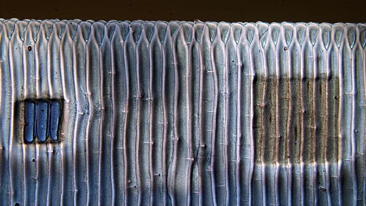
The other problem is that conductivity is not uniform: electricity travels far better along the extrusions and poorly between extrusion layers. In other words, the electrical properties are anisotropic — they are not the same in all directions.
While this doesn’t matter much when you’re 3D printing flat, 2D electrical traces, it becomes much more important when considering three dimensional electrical 3D prints. Imagine if the resistance levels varied along a complex 3D path!
For years researchers simply thought this effect was due to the geometry of the extrusions: just like mechanical strength follows the extrusion path, so do the electrical properties. Or do they?
The University of Nottingham researchers used advanced equipment to image the extrusions and discovered a different cause for the resistance.
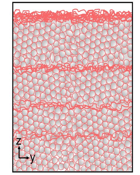
It turns out that the resistance is caused by organic residue leftover after the sintering process. They explain:
“These residues, which are added to the inks to help stabilise the nanomaterials, lead to the formation of low-conducting, very thin nanoscale layers which interfere with the electrical conductivity of the printed sample in the vertical direction.”
This is very good news, even though the discovery is only a research point. The new information will allow materials developers to reconsider the ingredients to their electrically conductive inks to ensure the conductivity is isotropic.
This means that in the future we could indeed see three dimensional conductive 3D printing, allowing the creation of many types of complex functional components not previously attempted.
Via The University of Nottingham