
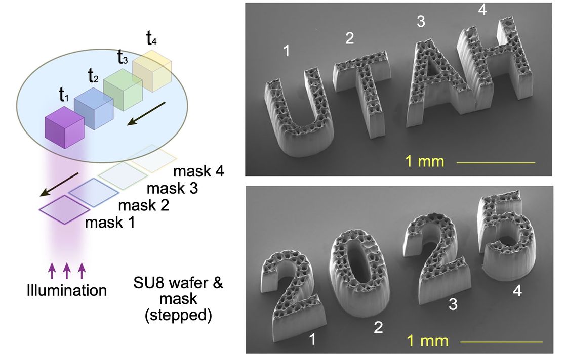
A University of Utah team has demonstrated a single exposure method for 3D printing intricate microstructures in roughly 20 seconds.
A Different Kind Of Volumetric Printing
Two-photon polymerization can produce extremely fine detail, but it writes point by point and can take hours to make millimeter-scale parts. Volumetric approaches such as computed axial lithography are far faster, but usually can’t achieve fine resolution.
The Utah researchers propose a new approach they call “single exposure holographic lithography”. Rather than building a part layer by layer, or scanning a laser through a resin vat, they use an inverse-designed phase mask to bend a 405nm laser beam into the required 3D light pattern inside a thick layer of SU-8 photoresist.
In other words, the optical mask is doing the work normally done by machine motion and slicing software. The mask compensates for diffraction so that the projected pattern remains sharp deep into the resin.
A conventional photomask rapidly loses contrast as the light propagates through thick resist, blurring small features. The inverse-designed mask maintained sufficient contrast through a 720 micrometer depth.
The team printed lattices, Penrose patterns, aperiodic “hat” tiles, and MEMS-like structures. Their hexagonal lattice measured 800 x 800 x 720 micrometers, with walls around 6 micrometers thick and an aspect ratio above 120:1.
Fast Exposure, Slower Reality
Their exposure time is certainly impressive: typically 20 seconds in total (!), with geometry-dependent exposures ranging from 12 to 32 seconds. The researchers estimate a rate of 0.36 million voxels per second, far ahead of the 10³ to 10⁴ voxels per second commonly associated with serial 2PP systems.
There is a catch, however. “Twenty seconds” covers only the exposure, not the whole production cycle. The SU-8 requires a lengthy bake before exposure, another two-hour post-exposure bake, and roughly 60 minutes of development. This is clearly not going to be a new form of desktop 3D printer waiting to happen.
The process also currently depends on custom-fabricated grayscale phase masks. Each mask is optimized for a specific geometry and for the optical properties of the resist. A material change, particularly one that alters refractive index or absorption, means reoptimizing the mask.
However, the researchers showed that stepping the substrate can tile repeated structures. A three-unit lattice was made in 68 seconds, including translation time between 20-second exposures. They suggest an automated setup could produce more than 4,000 structures per day.
That sounds promising for production of microfluidic parts, micro-optical elements, and architected materials, where a single mask could be reused many times. It is a lot less compelling for one-off custom parts, unless mask fabrication becomes dramatically simpler.
The Constraints Are Already Visible
As target depth rises, features broaden and contrast falls. At 6,400 micrometers of simulated depth, feature width increased from 6 to 16 micrometers. Dense patterns are also harder to form because optical side lobes begin to interfere with neighboring features. So there are some limits to this process.
Post-processing is another concern. Thin unsupported walls can deform during development, and deep internal channels are difficult to clear completely. In capillary flow tests, residual resist obstructed lower channels and limited liquid penetration. Longer development helped, but eventually caused delamination from the glass substrate.
The printed lattices did show useful behavior. Hollow channels wicked dyed water through capillary action, while compression tests measured an effective Young’s modulus of 5.7 GPa before buckling and collapse took over.
If the challenges can be overcome, this method could become an interesting complement to 2PP technology.