
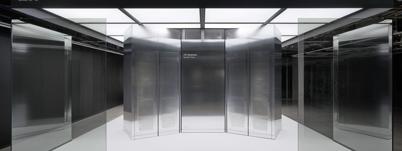
Charles R. Goulding and Preeti Sulibhavi discuss how advances in quantum computing may accelerate materials discovery, transform manufacturing processes, and create new opportunities for the additive manufacturing industry.
For decades, quantum computing was largely confined to university laboratories and government-funded research programs. While the technology captured headlines periodically, practical applications remained elusive and commercial investment was limited. Today, however, quantum computing is rapidly transitioning from a scientific curiosity to an emerging industry, and the implications could be significant for manufacturing, materials science, and ultimately the 3D printing sector.
Until the current decade, quantum computing research in the Western Hemisphere was concentrated primarily at leading universities and national laboratories. In the United States, institutions such as MIT and Caltech have been among the most prominent centers of quantum research. In Europe, organizations including Delft University of Technology in the Netherlands, along with Oxford and Cambridge in the United Kingdom, have produced much of the foundational work that underpins today’s quantum systems.
China has also invested heavily in quantum technologies, although the extent and progress of those efforts are often difficult to assess due to limited transparency. For many years, only a handful of major commercial firms were willing to commit the substantial resources required for long-term quantum development. IBM and Google were among the earliest corporate pioneers, investing billions of dollars in quantum hardware, software, and research infrastructure long before any clear commercial return was visible.
That situation is changing rapidly.
Why Is Global Investment Accelerating the Commercialization of Quantum Hardware?
The scale of the investment reflects a growing consensus that quantum computing has moved beyond basic research. Governments and industry leaders now view quantum technologies as potentially transformative for national security, economic competitiveness, advanced manufacturing, and scientific discovery.
This rapid transition of quantum computing from university laboratories into an industrial technology sector is driven by substantial federal funding and commercial scaling mandates:
- Federal Commercialization Grants: In May 2026, the U.S. government launched a US$2 billion commercialization initiative across nine quantum computing firms, including a US$1 billion grant to IBM for its Anderon quantum chip plant in New York and US$375 million to GlobalFoundries.
- The Complexity of the Quantum Stack: Beyond qubits, functional quantum supercomputing environments require the iterative engineering of localized control electronics, cryogenic systems, photonic devices, and advanced networking architectures.
- Interoperability and Open Ecosystems: Industry leaders are shifting away from rigid, vertically integrated platforms toward open, interoperable systems, as demonstrated by Cisco’s Universal Quantum Switch prototype designed to route quantum states across divergent hardware platforms.
Other recipients include D-Wave Quantum, Rigetti Computing, Infleqtion, Atom Computing, PsiQuantum, Quantinuum, and Diraq. The goal is to accelerate domestic manufacturing capacity and strengthen U.S. leadership in what is increasingly viewed as a strategic technology sector.
In June 2026, New York Tech Week attendees descended upon Manhattan to debate and educate about emerging technologies. IBM contributed to the conversation by hosting a panel to discuss, as its title suggested, “What Quantum Actually Means for Computing.” Jerry Chow, CTO of Quantum-Centric Supercomputing and IBM Fellow, took the stage before a packed auditorium at Big Blue’s One Madison Avenue office to debate the state and future of the field with speakers from academic partners that included New York University (NYU), Rensselaer Polytechnic Institute (RPI), and Stony Brook University.

Quantum computing requires a complex stack of technologies. While much of the public attention focuses on qubits, the quantum equivalent of classical bits, successful quantum systems also require specialized control electronics, cryogenic systems, photonic devices, software platforms, networking technologies, and advanced manufacturing processes.
This has led to an important debate within the industry. Should quantum computing be developed through vertically integrated platforms where a single company controls the entire technology stack, or through an ecosystem of specialized suppliers providing best-of-breed components?
Historically, the electronics industry has demonstrated the strengths of specialization. During the automation boom of the 1980s, the most successful manufacturing ecosystems often emerged when independent suppliers focused on solving specific technical challenges better than anyone else. However, today’s technology landscape is dominated by hyperscale companies with enormous financial resources. It is entirely possible that leading supply chain innovators will eventually be acquired by larger players seeking to control key technologies.
Vertical integration offers advantages in system optimization and compatibility, but it can also create one-size-fits-all solutions that may not be ideal for every application. The outcome of this debate will likely shape the structure of the quantum industry over the next decade.
Interestingly, recent developments suggest that interoperability may become increasingly important. In April 2026, Cisco announced its Universal Quantum Switch, a research prototype designed to connect quantum systems using different qubit technologies and encoding methods. Cisco’s approach reflects the view that the future quantum ecosystem will consist of multiple hardware platforms working together through standardized networking infrastructure rather than a single dominant architecture. The company demonstrated the ability to route quantum information among different systems while preserving quantum states, an important milestone toward large-scale quantum networks.
The potential applications of quantum computing are extensive. Researchers expect quantum systems to tackle computational problems that are effectively impossible for even the largest classical supercomputers. Areas frequently cited include molecular simulation, pharmaceutical development, advanced materials design, financial modeling, logistics optimization, climate analysis, and cryptography.
Materials science may prove particularly significant. Many manufacturing breakthroughs depend on understanding how atoms and molecules interact. Traditional computer simulations often struggle with these calculations because the complexity increases exponentially as systems become larger. Quantum computers, by contrast, are naturally suited to modeling quantum interactions.
This is where the connection to additive manufacturing becomes particularly interesting.
While quantum computing may seem far removed from 3D printing, the two technologies are already intersecting in several important ways.
One of the most immediate links is through the manufacturing of quantum hardware itself. Many quantum computing systems require highly specialized components with complex geometries that are difficult or impossible to fabricate using conventional methods. Additive manufacturing is increasingly being used to produce cryogenic hardware, microwave waveguides, photonic structures, vacuum components, and thermal management systems for quantum devices. Researchers at several quantum laboratories have adopted metal additive manufacturing to produce customized cryogenic assemblies used in superconducting quantum computers. The ability to rapidly iterate designs and optimize internal geometries has enabled engineers to reduce weight, improve thermal performance, and accelerate development cycles.

Photonic quantum computing companies are also exploring advanced additive manufacturing techniques. Firms such as PsiQuantum and others developing photonic architectures rely on increasingly complex optical components and packaging technologies. As photonic systems scale, additive manufacturing offers opportunities to produce intricate optical mounts, alignment fixtures, and integrated photonic packaging structures that would be expensive or impractical using traditional machining.
Additive manufacturing is also contributing to the development of quantum sensors and quantum networking hardware. The miniaturization and customization enabled by 3D printing can simplify the production of specialized enclosures, optical systems, and support structures used in experimental quantum devices.
The relationship extends beyond hardware production. One of the most promising long-term applications of quantum computing is the discovery of entirely new materials.
The additive manufacturing industry has spent years developing improved metal alloys, polymers, ceramics, and composite materials. Yet much of today’s materials development still relies on a combination of simulation, experimentation, and trial-and-error testing. Quantum computing could dramatically accelerate this process.
By simulating atomic interactions with unprecedented accuracy, future quantum systems may enable researchers to identify new materials specifically optimized for additive manufacturing processes. These could include stronger lightweight alloys, higher-temperature polymers, advanced battery materials, improved semiconductors, and entirely new classes of printable materials that do not yet exist.
The impact could be similar to what artificial intelligence is beginning to accomplish in materials discovery, but potentially on a much larger scale. Quantum-enhanced materials development could shorten research cycles from years to months and significantly reduce development costs.
It is still early days. Quantum computing faces substantial engineering challenges before large-scale commercial systems become commonplace. Error correction, qubit stability, manufacturing scalability, and cost remain significant hurdles. However, recent government investments, growing private sector participation, and advances in quantum networking suggest that the industry is entering a new phase.
For the additive manufacturing industry, quantum computing should not be viewed as a distant technology with little relevance to 3D printing. The two sectors are becoming increasingly interconnected through hardware production, advanced manufacturing methods, and next-generation materials development.
How Does Additive Manufacturing Drive Quantum Infrastructure Optimization?
Ultimately, to overcome the severe geometric and thermal constraints imposed by quantum mechanics, hardware developers utilize industrial 3D printing to fabricate mission-critical infrastructure:
- Custom Cryogenic and Vacuum Hardware: Superconducting quantum systems operate at ultra-low temperatures. Metal additive manufacturing allows engineers to print consolidated cryogenic assemblies and vacuum components that optimize internal flow geometries and reduce weight.
- Intricate Photonic Packaging: Photonic quantum computing firms, such as PsiQuantum, utilize advanced 3D printing to fabricate complex optical mounts, precise alignment fixtures, and integrated packaging structures that are impossible to machine via traditional methods.
- Quantum-Accelerated Materials Discovery: Future quantum systems are uniquely equipped to simulate atomic and molecular interactions with absolute precision. This capability will eliminate traditional trial-and-error testing, allowing researchers to discover novel high-strength alloys, ceramics, and printable polymers specifically optimized for additive manufacturing.
How Do Quantum Engineering Activities Align with Research and Development Tax Credit Criteria?
Synthesizing multi-functional hardware components, testing qubit containment parameters, and programming quantum switches involves resolving deep technological uncertainties, mapping directly to Section 41 R&D eligibility.
| Core R&D Technical Activity | IRS Four-Part Test Alignment | Financial Recovery Impact |
| Cryogenic Component Consolidation | Resolves mechanical and thermodynamic uncertainty regarding thermal dissipation and internal geometric optimization in 3D-printed metal assemblies. | Captures qualified internal labor hours spent modeling complex internal channels and programming multi-axis laser toolpaths. |
| Photonic Alignment Optimization | Conducts a systematic process of experimentation to design micro-machined optical mounts that maintain sub-micron alignment tolerances. | Recovers the direct payroll costs of optical, mechanical, and materials systems engineers executing pre-production testing. |
| Interoperable Network Switch Engineering | Overcomes technological barriers associated with routing quantum information across distinct qubit architectures while preserving exact quantum states. | Offsets software development and systems configuration expenditures consumed during structural network simulation trials. |
Strategic Insight for CFOs and Technical Directors: While massive commercialization grants under federal initiatives infuse immediate capital into the quantum landscape, the Section 41 R&D Tax Credit provides an ongoing, sustainable mechanism for cash-flow recovery. Because 3D printing and advanced component validation are direct indicators of qualifying R&D activity, firms developing quantum hardware can systematically recover a significant percentage of internal engineering wages and prototype material costs. Partnering with R&D Tax Savers ensures that these multi-layered technical expenses are robustly documented to withstand strict IRS scrutiny.
A Quantum Leap
As quantum computing continues its transition from research laboratories into commercial deployment, developments in the field will likely have a growing impact on additive manufacturing. Companies involved in materials development, advanced manufacturing systems, and industrial innovation would be wise to keep a close eye on this emerging technology.