
A new research paper suggests additive manufacturing is moving steadily toward producing complete functional electronic devices.
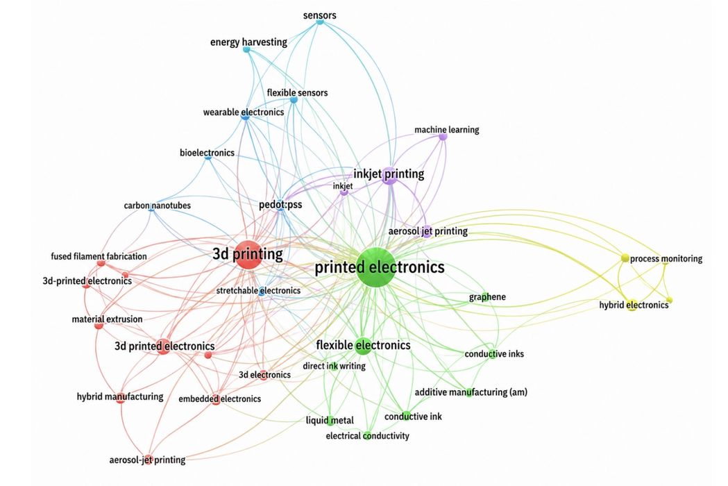
Researchers from institutions in Taiwan, China and Australia examined the state of additive manufacturing for electronics, including materials, processes, applications and commercialization challenges. Their review covers developments through 2025 and includes a bibliometric analysis of 465 Scopus publications.
The basic idea is pretty compelling. Instead of 3D printing a plastic housing and later installing a conventional circuit board, additive processes could fabricate structural, conductive, dielectric and even active elements as parts of the same manufacturing sequence.
That could enable electronics with shapes impossible to produce using conventional planar PCB manufacturing. Think curved antennas, embedded sensors, wearable devices, unusual battery geometries and electronics conforming directly to mechanical parts.
Many Processes, Many Possibilities
The researchers examined five major AM process families: material extrusion, vat photopolymerization, material jetting, binder jetting and powder bed fusion. Each has different strengths, and there clearly isn’t a single obvious process destined to dominate electronic additive manufacturing.
FFF, for example, can print structural components using conventional thermoplastics while conductive composite filaments can provide electrical functionality. Direct ink writing extends extrusion toward flexible electronics by depositing conductive and functional inks.
Vat photopolymerization offers considerably finer resolution. The review describes DLP fabricated conductive hydrogels used in flexible pressure and strain sensors, including structures patterned at approximately 150 microns.
Material jetting is particularly interesting because multiple inks can potentially be deposited with very fine control. Researchers have already demonstrated conductive traces, dielectric layers, biomedical sensors and complex RF components. One cited metasurface included seven integrated metal layers with internal vias.
There are also hybrid approaches. SLS can produce a complex polymer substrate, after which aerosol jet and screen printing add conductive interconnects and sensing materials. That combination allows electronics to follow freeform 3D surfaces rather than remaining trapped on flat circuit boards.
The Manufacturing Gap
This sounds great, but the review identifies the same problem that appears repeatedly with advanced AM research: scaling it.
Conductive printed materials frequently perform below their traditional counterparts. One cited gold nanoparticle ink achieved only 16 percent of bulk gold conductivity. Nozzle clogging, ink wetting, interlayer adhesion, anisotropy, porosity and material compatibility can further affect reliability.
Then there is throughput.
The researchers classify current electronic AM technologies primarily at prototype stage, roughly TRL four through seven. Manufacturing costs can be competitive for prototypes and low volume production, but remain high for mass production. Throughput is also below conventional electronics manufacturing.
Standards are another obstacle. ISO/ASTM 52900 provides general AM terminology, while electronics specific standards are still emerging. Long term electrical, mechanical and electromagnetic reliability data will be essential before aerospace, medical and other regulated industries become comfortable using these processes.
The review points toward several directions that could change this equation: true multi material printing, nanoscale fabrication, 4D printed responsive electronics, and integration with AI and IoT systems. Multi material systems could be particularly significant because conductors, dielectrics and active materials might eventually emerge from a single coordinated build.
Whether these technologies can move out of the laboratory and retaining conductivity, reliability and reasonable production economics is a big question.
Via The International Journal of Advanced Manufacturing Technology