
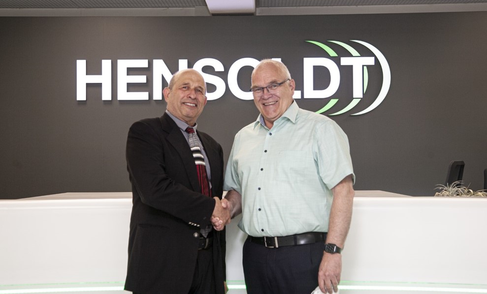
Meet J.A.M.E.S., a new joint venture between Nano Dimension and HENSOLDT.
J.A.M.E.S. spells out what it’s all about: Jetted Additively Manufactured Electronics Sources.
The focus on 3D printing electronics jives well with what Israel-based Nano Dimension has long been known for, but its partner company may be a bit less well-known to those primarily familiar with additive manufacturing companies. HENSOLDT is a German company headlining itself as the “Sensor Solutions House” on its company About Us page. The focus is on high-tech defense and security electronics, as well as military and civilian sensor solutions.
HENSOLDT has also been using 3D printing technology from Nano Dimension since 2018. In 2019, we heard a bit about Nano Dimension, HENSOLDT, and TTM working as strategic partners “making great plans” to address Tier 1 research for the Department of Defense. We also heard that year about HENSOLDT housing the first installation of Nano Dimension’s LDM (Lights-Out Digital Manufacturing) system.
Now, the companies deepen their journey together through J.A.M.E.S. The AME (Additively Manufactured Electronics) focus is important to the teams’ work for a number of reasons, as they explain:
“AME is a highly agile and customized method for development, prototyping and fabrication of electronic circuits, which results in a significant reduction of time and cost in the time-to-market process. In addition, AME delivers a verified design before production begins, resulting in a higher quality product.”
A co-invested $6 million forms the Taufkirchen, Germany-based JV. The primary goal, they explain, is to develop “an electronic designer’s community that will exchange designs and methodologies for manufacturing, component integration, and materials for Printed Electronics (PE) and Additively Manufactured Electronics (AME). By connecting the complete value chain of all designers and users-of-designs across corporate and geographical borders, J.A.M.E.S will allow members of its community to develop, prototype, market, and trade AME and PE designs, proof of concepts, and products.”
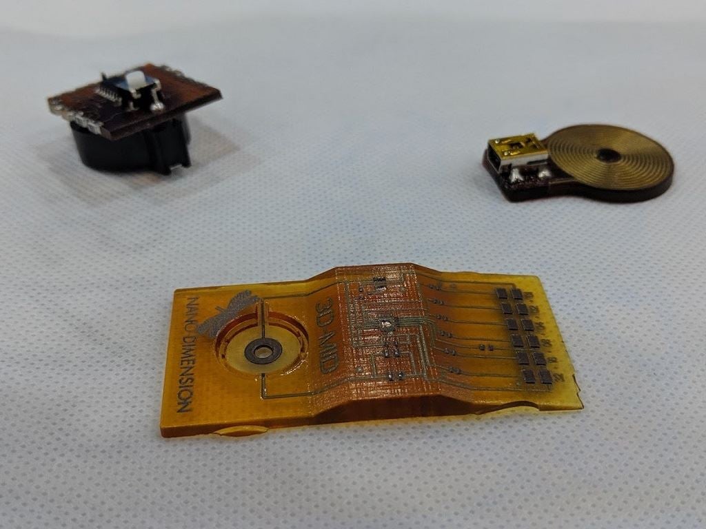
“HENSOLDT, as a market leader in the field of sensor technology and optronics, expects the closer cooperation with Nano Dimension to accelerate development cycles as well as spare parts production to respond to customer needs more quickly and cost-effectively. Using special dielectric and conductive nanoparticle inks, it is now possible to design electrical components directly via the printer and bring them into a three-dimensional form,” said Marian Rachow, Head of HENSOLDT Ventures, who will serve on the J.A.M.E.S Board of Directors.
“HENSOLDT has been investing in basic research of digital 3D printing of electronic components for several years to make the benefits of this technology available for its own development and production. For example, in collaboration with Nano Dimension, HENSOLDT has already printed the world’s first 10-layer PCB, which carries soldered high-performance electronic structures on both outer sides, using a newly developed polymer ink from Nano Dimension. Increasing competition and accelerated customer procurement timelines will be one of the biggest challenges for established providers in the future. Our joint venture, J.A.M.E.S, not only offers rapid development of technology as a real alternative to conventional electronics manufacturing, but also offers small and medium-sized companies the opportunity to efficiently design new products.”
J.A.M.E.S. is set to build a cloud-based platform as well as an operating fablab for community experimentation and support. The community basis for the new joint venture is certainly intriguing. Prototyping services and support focusing on AME applications may be a nice boost to the creation and eventual wider-spread adoption of 3D printing in electronics.
“The newly formed J.A.M.E.S is focused on building a cloud-based platform. In the future, other companies and customers are expected to upload a wide variety of electronic components in their usual CAD/CAM/CAE software and convert them into a new type of AME file on the platform. Furthermore, they will be able to obtain additional designs via the described platform, modify them, add their own form factor and have them printed on-demand,” said Yoav Stern, Chairman of the Board and CEO of Nano Dimension, who will serve as the Chairman of the J.A.M.E.S Board of Directors.
Via Nano Dimension and HENSOLDT