

Researchers have developed a technique to fabricate tiny 3D objects using an unusual molecular force.
The force involved is the Van der Waals force, a peculiar set of forces that provide attraction and repulsion between atoms and molecules due to polarizations in particles. This is quite different from the normal chemical bonds that hold materials together, and is notably weaker.
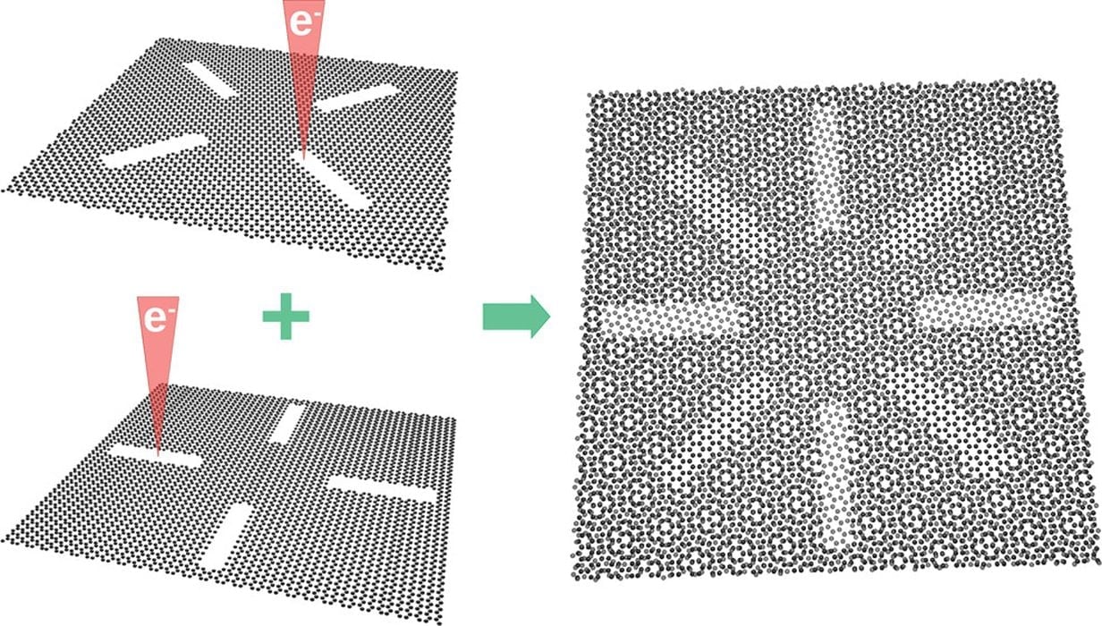
The researchers were able to stack layers of 2D materials made through electron etching with a lateral accuracy of only 10nm. The layers were “attached” using only Van der Waals forces, rather than chemical bonds.
The interesting part is that the layers can be of arbitrary design, and this opens up many possibilities for new types of metamaterial development. They explain:
“Importantly, these layers can be assembled in any arbitrary sequence, yielding so-called van der Waals (vdW) heterostructures. This allows combining the properties of the constituent layers, and may also lead to unique features due to the interaction between the layers. For example, hexagonal boron nitride (hBN) is not only an excellent substrate for graphene, but can also have a profound influence on graphene’s electronic properties that sensitively depends on the relative alignment of the sheets.”
How exactly is this done? They explain further:
“In this work, we developed an approach that combines the high-resolution, electron-beam based structure definition in free-standing 2D material membranes with the assembly of prestructured layers into van der Waals heterostructures. A structure is defined in every one- or few-atom thin layer, and the layers are placed on top of each other with a precise lateral alignment. We categorize this as a form of 3D printing, which (in most of its implementations) also proceeds by forming a target structure layer by layer, and with a chosen arbitrary structure in each individual layer. Critically, the lateral alignment between the layers must be of a similar accuracy than the targeted resolution. Here, we repeatedly achieve an accuracy of about 10 nm, which is given by limitations of the SEM stage control during manual stacking, and probably is not the fundamental limitation of the approach. We also point out that the material for each layer can, in principle, be chosen from the vast repertoire of available 2D materials, which should make it possible to directly create functional devices.”
The last sentence tells of the potential of this approach: “directly create functional devices”.
While this sounds quite amazing, it does require very specialized equipment to be accomplished, including electron microscopes, etching equipment, and it must be performed in a vacuum.
These are significant challenges to commercialization, but as this is research there could be considerable optimization yet to be done. In the end one can only imagine the types of microscopic devices that might be produced by this unusual approach.
Via ACS