
A newly published Taiwanese patent describes a powderless metal additive manufacturing concept using a TFT backplane to electrochemically print metal.
The filing describes an “electronic printing device” that patterns metal from an electrolyte onto a separate cathode plate by addressing millions of tiny anodes on a thin-film transistor (TFT) substrate.
Unlike laser powder bed fusion or binder jetting, this approach avoids metal powder, inert gas handling, and sintering, targeting instead for low-cost, highly parallel deposition driven by mature display-style electronics.
Similar ideas have circulated in electrochemical additive manufacturing, notably at startups championing copper deposition without powders, but this patent pushes the concept further by borrowing pixel-driving circuitry straight from flat-panel displays.
There is one company known to be 3D printing with an electrochemical process, Fabric8Labs. It is not clear whether this new patent overlaps with their process.
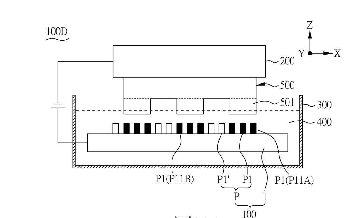
In the proposed system, the printing substrate sits in an electrolyte opposite a cathode plate. Scan and data lines route signals to per-pixel driver circuits, described as a two transistor, one capacitor (2T1C) cell, switching “printing units” on and off. Energized units locally promote reduction of metal ions so metal deposits on the opposing cathode at matching locations. By energizing different pixel groups over multiple passes, the system grows features in steps, eventually forming fully 3D metal parts.
TFT Backplane Controls Electrochemical Deposition
The patent’s key concept is the backplane structure and its robustness in a wet, corrosive environment. Each pixel includes a conductive layer with two thickness zones: a covered first portion and an exposed second portion. The first portion is deliberately thicker than the second (e.g., thickness difference on the order of ten to 1000 nm). That thickness step is created after patterning the insulating stack, which the authors say removes etch byproducts and improves reliability.
The anode sits in an opening above the thinner, exposed region and contacts it. Multiple inorganic and organic insulating layers, plus optional protective coatings over the periphery, are meant to keep moisture and ions out of the electronics. A grid-shaped power distribution network reduces line impedance across the active area, a familiar tactic from display engineering to maintain uniform drive and current.
The chemistry is straightforward: the electrolyte can contain common plating metals such as copper, nickel, silver, gold, tin, zinc, tungsten, cobalt, or combinations. The cathode plate might be copper, carbon, or other conductive materials. The document suggests sequential energizing of pixel groups to build stacked features, implying a quasi-layered growth model without moving nozzles or lasers. In theory, the parallelism could be enormous, with every pixel acting as a tiny, software-defined tool.
Promise And Practical Constraints
Two claims are immediately interesting: cost and throughput. Replacing lasers and powders with a TFT substrate, thin-film stacks, and a plating bath could enormously reduce capital expense, while display-style manufacturing might scale area quickly. At full TFT aperture, pixel-by-pixel control could deliver extreme parallelization and potentially very fine resolution.
However, key constraints remain unaddressed in the patent. The patent does not specify resolution, pixel size, build area, deposition rate, or final part properties, although those likely depend on the specifid TFT panels used. Building true 3D geometry from a flat cathode raises questions: how tall can features grow before shielding, mass transport limits, and stress cause quality issues, and how are supports or overhangs built? Post-processing, such as part release from the cathode, rinsing, and any required surface finishing, is also not specifically mentioned. Reliability of the backplane under prolonged immersion and voltage cycling, despite the protective stacks, could be a major hurdle.
Nevertheless, making the pixel array as a “toolhead” is really clever. It leverages decades of TFT backplane know-how — scan drivers, storage capacitors, and low-impedance power meshes — to enable maskless, reconfigurable metal deposition. If it works, it could serve service bureaus and labs needing fast, low-cost copper or nickel structures, and potentially complement PCB, RF, or thermal management applications where dense, patterned metal is essential.
One challenge to this approach is that only metals suitable for electroplating will work. Some metals, particularly aluminum, titanium, magnesium, and some steels, all oxidize instantly, making them troublesome for electroplating, and therefore this method as well.
We should now watch for includes prototype panels, benchmark parts, and hard numbers for feature size, layer increment per pass, and deposition throughput. Also important will be backplane lifetime in electrolyte, sealing effectiveness, and any closed-loop sensing for uniformity. If the team can demonstrate consistent growth through millimeters without severe defects, adoption could follow quickly, given the supply-chain maturity of display manufacturing.
If all that succeeds, we may have just seen an entirely new way to 3D print metal.
Via Google Patents