
Researchers have embedded working multilayer strain sensors inside LPBF titanium, suggesting that self-monitoring metal parts are getting closer.
Embedding sensors into metals during Laser Powder Bed Fusion (LPBF) has long been prevented by heat. Polymer dielectrics and adhesives tend to char or delaminate under high temperatures, which is why most tests have used stainless steels or nickel alloys and often resort to cavities, coatings, or post-fit assemblies. Titanium, particularly Ti-6Al-4V, makes it even more challenging with low thermal conductivity and demanding process windows, yet its relevance in aerospace and implants makes it the material that could best use embedded sensors.
A team from Argonne National Laboratory, University College London and the University of Sheffield reports a way that might just work. Their approach combines direct ink writing (DIW) of conductive traces with a carefully tuned polymer dielectric and a powder-mediated thermal shield applied before the top skin is fused. The result is a strain-sensing architecture that rides safely through the LPBF cycle and remains electrically functional when the part comes off the print plate.
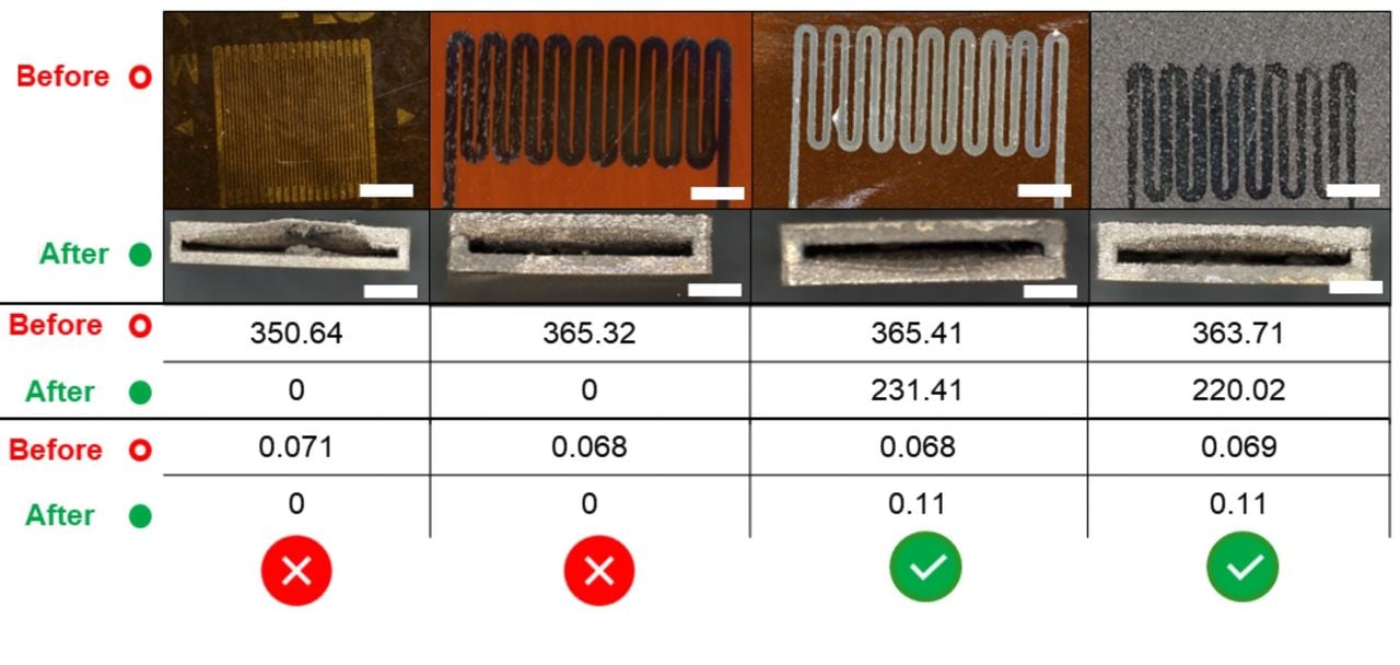
Their sensor concept centers on a thin dielectric of tripropylene glycol diacrylate (TPGDA) — chosen for roll-to-roll compatibility and moderate thermal stability — topped with DIW-printed traces from a silver nanoparticle ink. The team optimized the dielectric surface via low-current plasma to balance wettability and smoothness for clean line definition, achieving feature sizes near ten micrometers using custom-pulled glass nozzles. Thermal constraints were figured out in advance: polymer degradation accelerated above about 200C. Ink curing at 150C for 3,800 seconds yielded stable conductivity around 350 ohms without damaging the dielectric.
To survive the LPBF cycle, the researchers spread a one mm layer of Ti-6Al-4V powder over the printed gauge before scanning the closure wall. Finite element modeling indicated melt pool temperatures soar locally, but the thermals decay within the powder bed; by the time it reaches the embedded device, temperatures near the gauge were modeled at about 25C. Parts were printed on an Aconity Lab system under argon using 190 W power and 1.2 m/s scan speed.
Four architectures were tested: commercial foil on polyimide (PI), DIW on PI, DIW on glass fiber reinforced phenolic, and DIW on TPGDA. The PI-backed options struggled, likely from interfacial stresses and adhesive degradation under rapid heating and cooling. In contrast, the phenolic and TPGDA-backed gauges emerged intact and functional. Resistance dropped after embedding by roughly 134–144 ohms, consistent with additional sintering of the silver network during the brief thermal excursion. Three-point bending showed preserved strain sensitivity, with a slight gauge factor increase after embedding.
The result is a procedure that seems to work: DIW for patterning, a controllable dielectric, and a simple but effective powder barrier. This could be a potential way to integrate sensing without sacrificing build volume or resorting to complex inserts. The workflow could be appealing to aerospace teams looking for structural monitoring, as well as research groups prototyping smart fixtures and tooling.
The use of roll-to-roll TPGDA suggests a scalable path for dielectric films, and DIW is already familiar to labs building bespoke electronics. Wiring and data acquisition were demonstrated via a Wheatstone bridge and low-cost electronics, hinting that instrumentation need not be exotic.
If this method survives commercialization, we could have structures and more importantly, aircraft, that provide far more accurate information about part performance. That should translate into more reliable and safe air travel.
Via OpenAlex